WaferGuard ML
Sprint 1: WM811K Dataset Exploration
2026-02-01
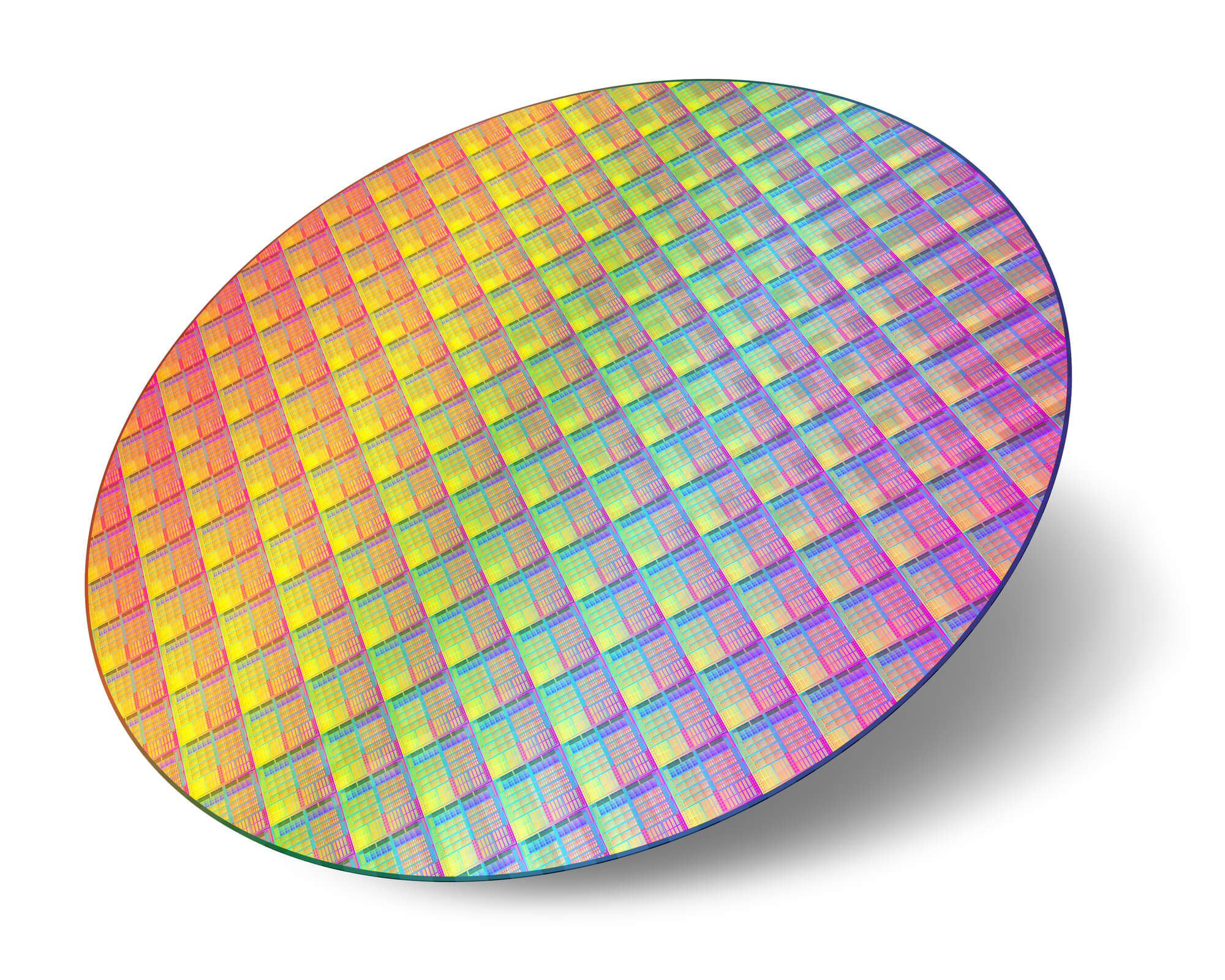
What is a Semiconductor Wafer?
A semiconductor wafer is a thin, circular slice of silicon used to manufacture computer chips.
- Thin circular disk (like a CD, but 12 inches wide)
- Pure silicon crystal grown in labs
- Hundreds of transistors per mm²
Silicon wafer = computer chip foundation
The Challenge
- Traditional manual inspection is slow and inconsistent
- Defects detected too late in production
- Lost productivity = Millions in yield loss
- Need real-time, automated detection
Wafer Images Dataset
- The data shape is 52×52.
- 0 means blank spot
- 1 represents normal die that passed the electrical test
- 2 represents broken die that failed the electrical test.
- These wafer maps are obtained by testing the electrical performance of each die on the wafer through test probes.
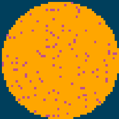
Example of a Normal Wafer
![]()
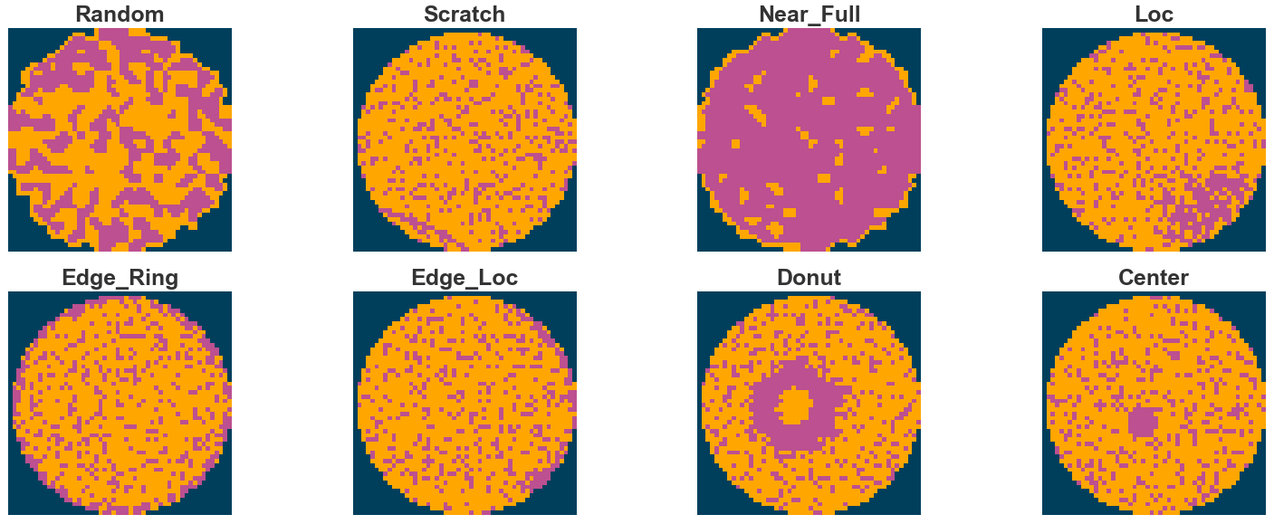
Defect Patterns
8 distinct defect categories analyzed in our dataset ![]()
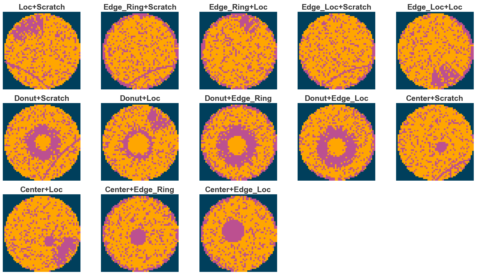
Two Types of Multi-Defect Patterns
![]()
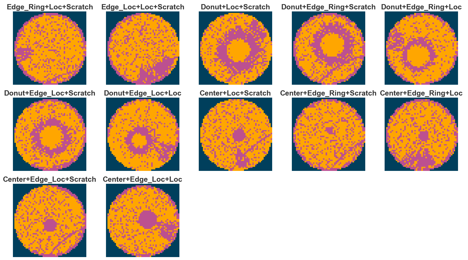
Three Types of Multi-Defect Patterns
![]()
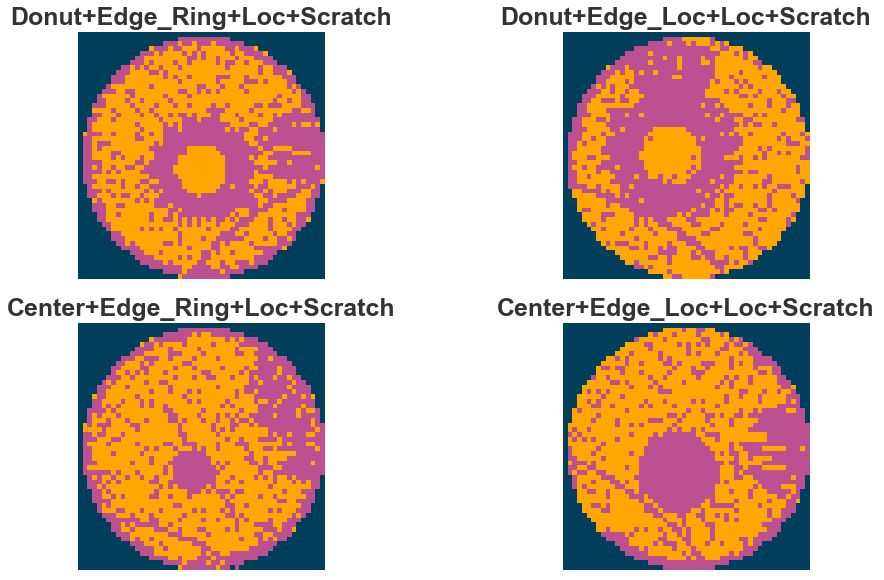
Four Types of Multi-Defect Patterns
![]()
Defect Pattern Labels
- The labels in the data are using one-hot encoding, a total of 8 dimensions, corresponding to the 8 basic types of wafer map defects (single defect).
- Normal: [0, 0, 0, 0, 0, 0, 0, 0]
- Center: [1, 0, 0, 0, 0, 0, 0, 0]
- Donut: [0, 1, 0, 0, 0, 0, 0, 0]
- Edge-Loc: [0, 0, 1, 0, 0, 0, 0, 0]
- Center-Donut-Edge-Loc: [1, 1, 1, 0, 0, 0, 0, 0]
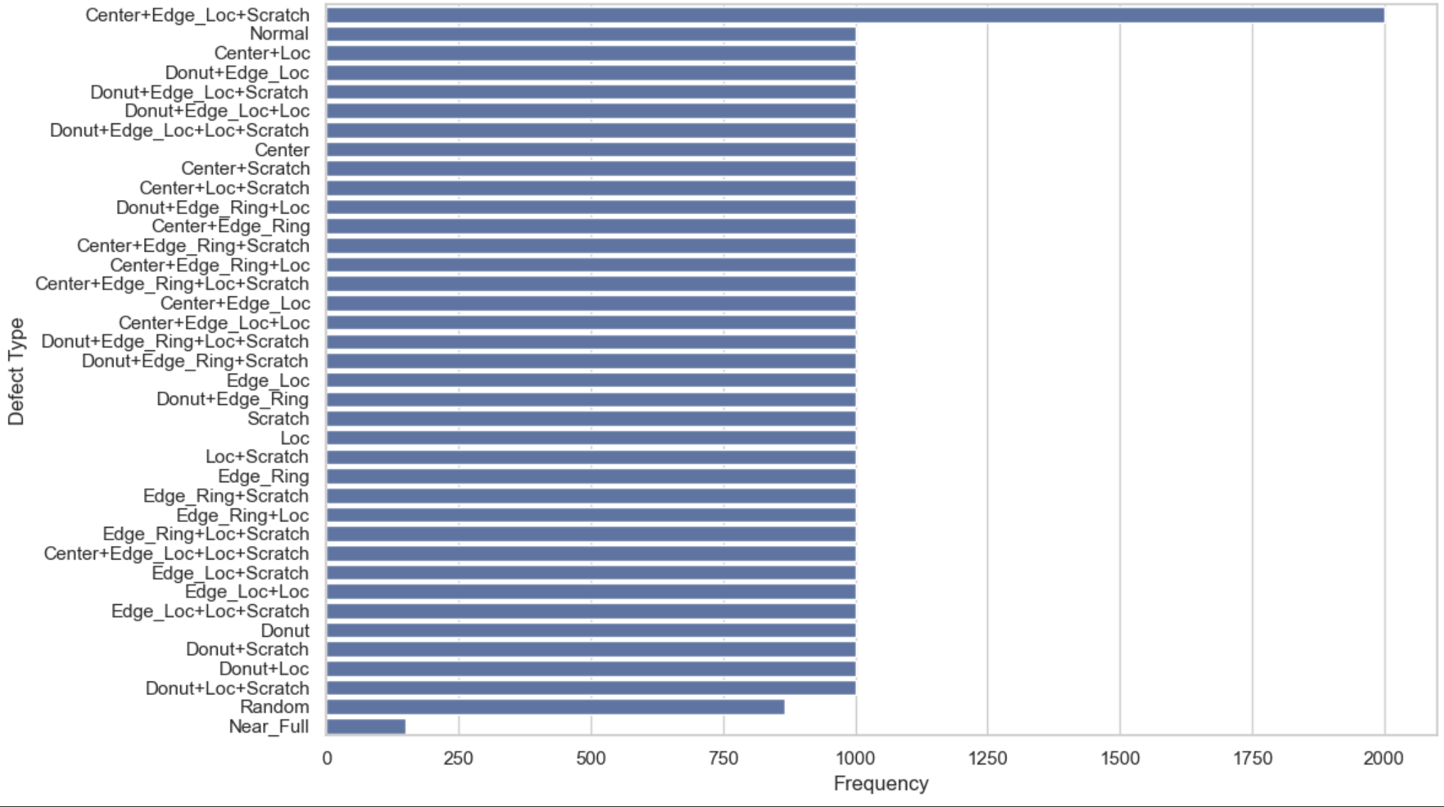
Pattern Distribution
![]()
Dataset Summary
- 38K Wafer Maps
- 52x52 Pixel Resolution
- One-Hot Encoded Pattern Labels
- 38 types in the mixed-type wafer map defect dataset
- 1 normal type
- 8 single defect types
- 29 mixed-type (2: 13, 3: 12, 4: 4) defect types.
Data Quality: Excellent
- No missing values
- Complete Coverage of Defect Types
- Mostly Balanced Classes
- Ready for Modeling